Implementation
Physical Implementation
- Synthesis for area & timing optimization
- SDC clean-up for constraint error fixes
- Static Timing Analysis — setup, hold, max transition & noise
- Simulation for functional verification
- Test vector generation
㈜스타칩스는 2024년 9월, ASIC 전문 업체로 법인 설립되었습니다.
Fabless와 Foundry를 위한 ASIC 전문 기술 업체입니다.
180nm에서부터 7nm Deep sub-micron까지의 풍부한 경험을 가진 엔지니어들로 구성되어 있으며, ASIC Design Service의 선두 주자로 나아갈 것입니다.
다수의 국내 반도체 회사와 설계 협력 관계를 구축하여, Fabless IC 고객사들에게 Non-Stop & One Time Success를 제공하는 최고의 반도체 기술 회사가 되고자 최선을 다하겠습니다.
반도체 설계 엔지니어의 동반자로서, 또한 반도체 개발·양산 지원의 Leader로서 반도체 업체들의 수익과 성장에 밑바탕이 되어드리겠습니다.
180nm — 7nm · Deep Sub-Micron
RTL 입력부터 최종 GDS 전달까지 12단계의 표준 ASIC 설계 흐름을 일관되게 수행합니다.
Capture the design using a hardware description language (HDL) or schematic entry.
Produce a gate-level netlist — logic cells and the nets connecting them.
Insert test logic for logic cells, memory, and IP.
Verify the gate-level netlist functions correctly.
Arrange the blocks of the netlist on the chip.
Decide the locations of cells within a block.
Insert buffers and inverters along the clock paths to balance clock delay.
Make the connections between cells and blocks.
Ensure the layout works as intended — design rule check (DRC) and layout-versus-schematic (LVS).
Check static and dynamic voltage drop across the power grid.
Confirm the design still works with the added loads of the interconnect.
Deliver GDS (Graphic Database System) to the process.
Implementation

Place & Route

DFT
다수의 국내 반도체 회사 및 글로벌 파운드리 공정 경험을 보유하고 있습니다.




ASIC 설계 의뢰와 협력 제안을 환영합니다. 편하게 연락 주세요.
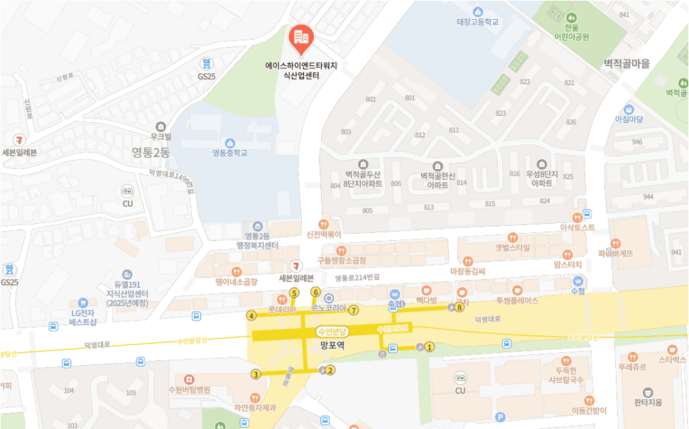
Address
경기도 수원시 영통구 영통로 237, 613호 (신동, 에이스 하이엔드타워 영통)
Tel
031-202-1277Fax
031-202-1288